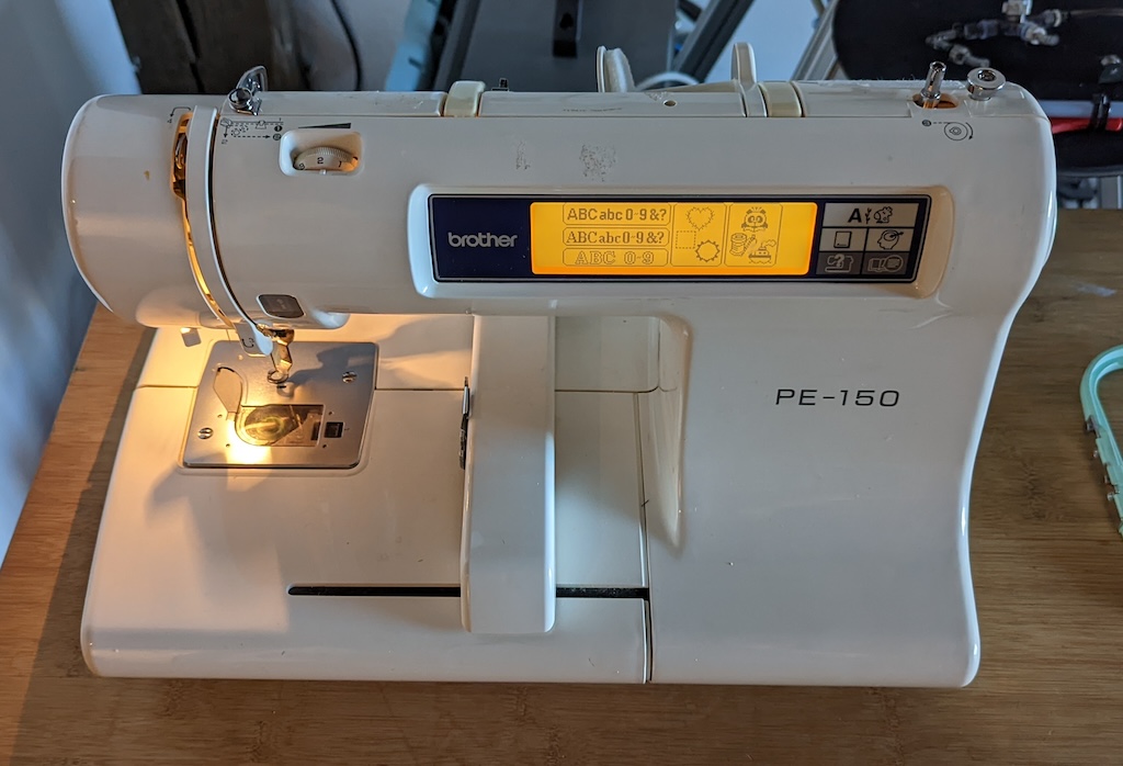
The Brother PE-150 is an old and affordable computerized embroidery machine. This kind of embroidery machine is pretty much just a sewing machine that can move the fabric around precisely according to instructions in a computer so the stitches it makes form predetermined patterns.

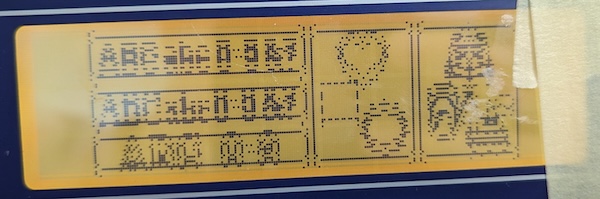
It has a satisfying amber LCD screen with a touch interface. There are many different patterns that are baked into it, like the smiling sun above.
I want to make designs on my computer using software like PEmbroider and then send them to the PE-150. But out of the box the only way to do that is with CompactFlash (CF) cards and proprietary software that is more expensive than the machine itself. So instead I’m going to take the machine apart and figure out how it works, and then design a new controller which runs my own software that can read instructions in whatever formats I care to implement.
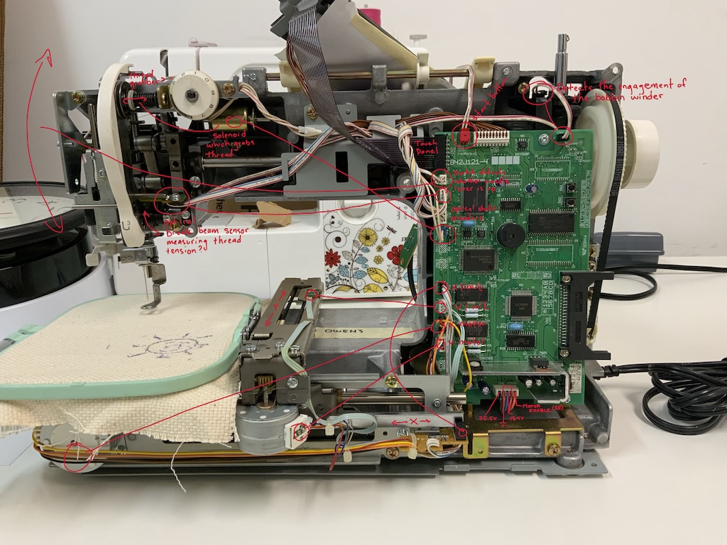
About a year ago during my first RC batch I took the first steps by disassembling the machine and poking around to see what I could figure out. There is quite a lot going on in there!
Some observations:
The controller could be replaced just by understanding how the downstream parts govern the behavior of the machine. But let’s see what we can understand about it just for the sake of curiosity.
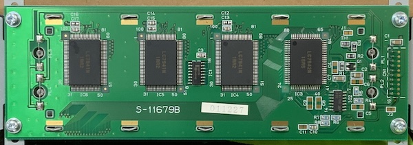
There are a bunch of connectors at the edges, which are labeled on the silk screen. Here’s what I think they do:
| Connector | Wire Count | Function |
|---|---|---|
| CN1 | 5 | Power and main motor control. From left to right: 25.5V, ground, 13.4V, ground, motor enable (5V). |
| CN3 | ? | CF card. |
| CN4 | 2 | Switch that detects when the bobbin winder is engaged. |
| CN5 | 10 | LCD. |
| CN8 | 2 | Switch that detects whether needle lever is up. |
| CN9 | 3 | Break beam sensor for measuring thread tension(?). |
| CN10 | 5 | Three break beam sensors. One for an optical encoder, and then two for interrupters that wrap partially around the main shaft. |
| CN11 | 2 | Thread grabber solenoid. |
| CN14 | 3 | X axis break beam limit sensor. |
| CN15 | 3 | Y axis break beam limit sensor. |
| CN16 | 4 | X motor. |
| CN17 | 4 | Y motor. |
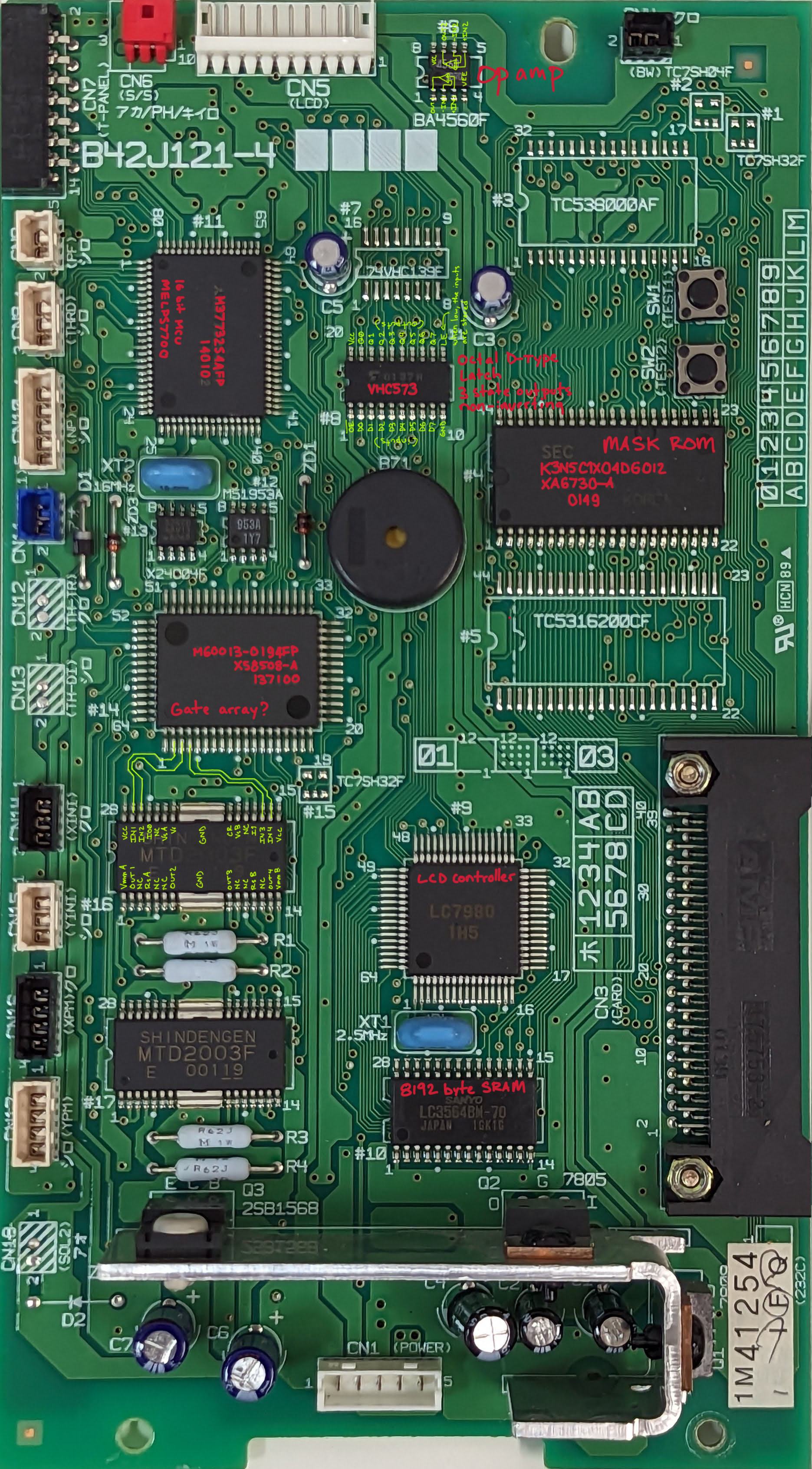
Moving inwards, let’s take a tour of the chips. What should we expect to find? There must be some kind of computer that is orchestrating the whole show. And this is an old machine, so we might find that it is made up of multiple chips that need to work together instead of an SoC with everything integrated. In that case there would be an MCU, some RAM for keeping track of different temporary results, some ROM to store the code and built-in stuff like LCD graphics/fonts and designs. We also know there’s an LCD and a touch screen, so there might be controller chips for those things. Ditto for the CF card interface. And there will need to be motor drivers for the XY gantry. Some sort of electronically controlled switch is needed to turn the big drive shaft motor on and off. Finally, miscellaneous electronics will be needed for getting whatever supply voltages are needed and conditioning various signals.
So what do we actually find? Some surprises! Here are the chips and my guesses about their roles:
| Chip | Role | Comments |
|---|---|---|
| M37732S4FP | 16 bit Microcontroller | The star of the show. “This microcomputer is suitable for office, business, and industrial equipment controller that require high-speed processing of large data.” |
| K3N5C1X04D6012 | Mask ROM? | No datasheet found using the number on the chip. The identical unpopulated footprint below it is labeled as TC5316200CF, which is a 2Mx8 Mask ROM. And it looks like some of the traces extend to the CF card connector, which would make sense if this is a memory interface. So the guess is that there is an option to have two ROMs but only one is populated, and these might each be an addressable memory bank along with the CF card. So no extra controller for the CF card is needed (or found). |
| M60013-0194FP | Gate array? | No datasheet found. It’s connected to the stepper motor drivers and various other things so it’s probably used to help implement IO logic. |
| MTD2003F | Stepper Motor Driver | Vm max 30V, 1.2A per phase, 3W power dissipation. One for each of the two XY gantry stepper motors. |
| LC7980 | Controller for Dot-matrix Graphic Display | “The LC7980 is a controller LSI for the liquid crystal dot matrix display. It stores display data sent from the 8-bit microcomputer in the display RAM attached externally and generates dot matrix LC drive signals.” |
| LC3564BM-70 | 8192-word x 8-bit SRAM | This is most likely the display RAM since it is right below the LCD controller and connected to it |
| BA4560 | Low Noise Op Amp | I didn’t trace this out but maybe it is for reading the resistive touch screen? Can’t see another potential signal needing buffering/amplification and it’s in the area where the connectors for the screen are. |
| MC14017B | Decade Counter | I didn’t trace this out but maybe it has to do with keeping track of the position from the optical encoder on the shaft. |
| LM7805 | Voltage Regulator | Takes in the 13.5V and outputs 5V for the digital logic. |
| 2SB1568 | PNP Darlington Power Transistor | Something to do with the steppers? Not sure yet. |
Everything except the screen is very simple - switches and motors (ignoring the CF card interface since I’m not going to use that). The screen is a graphical LCD with a resistive touch panel on top.
Getting the touch screen working shouldn’t be too bad so I am going to ignore it until a later stage. Maybe I’ll describe the details in a future post after I’ve dug into it. But I expect that it works something like keyboard matrices do. It’s not like a touch screen on a modern smartphone where you can get the exact position of multiple fingers, instead there is a discrete grid of touch switches. The controller will just figure out which one of these switches you’ve touched. In a keyboard this is usually done by having a grid of signals which are connected at the crossing points when a key is pressed. The controller scans through them by activating one row at a time and seeing which column input goes high. Then it knows the key at that row and column is pressed. The 15 conductors in the ribbon cable for this touch screen are probably used like that and I’ll be able to map them out for use later.
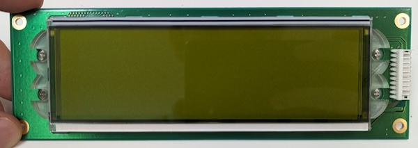
Now onto the fun part, displaying graphics!
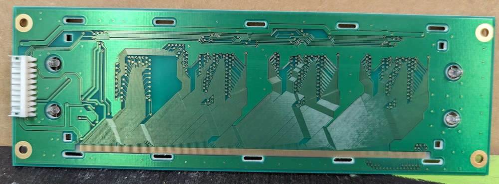
The output side of the screen is a lot more complicated. On the back there are 4 big chips which we can assume run the show. The connector for that PCB has 10 conductors, so we can assume that the graphics that the controller wants to be shown must somehow flow through those wires to these 4 big chips and then they translate them into the actual drive signals for the LCD.
The LCD actually also works kind of like the touch screen in the sense that there are rows and columns and you get something to happen at a particular spot by doing something with the row and column that intersect at that spot.
Here I took the glass part off of the screen so we can see the traces that connect to it underneath. You can see there are very many traces which all terminate in a row of vertical copper lines at the bottom where they will be connected up to the display glass via a squishy conductive bus (I guess this is some kind of stack of independent columns made of carbon-impregnated rubber?).
Inside the glass there are also electrical traces which are made of a material like Indium Tin Oxide (ITO), which is transparent but also conductive. Those traces go to the actual pixel cells which have liquid crystal squished in them. When a column and row are driven an electric field is formed in that little space which causes the liquid crystal molecules to rotate and change the polarization of light coming through. If it’s rotated such that it gets filtered out in another part of the screen then we see that pixel as black.
When I took it all the way apart the first time I put it back together with the rubber connector between the PCB and the glass part of the display shifted a little bit. So some of the drive signals didn’t get there, and some of them drove an extra row or column. Resulting in the dead or shifted lines / pixels you see here.
So how do the 10 signals coming in over that connector turn into the bazillion signals going to the rows and columns of pixels in the glass part? To answer that we need to figure out what those big chips are doing.
The three on the left are the same part, the LC7941ND dot-matrix LCD driver. The last one on the right (closest to the connector) is an LC7942ND, which is also a dot-matrix LCD driver. These are members of a little family of parts from Sanyo which are intended to work together to drive a display like this. The LC7980 that we saw on the controller PCB above is also a member of this family.
From reading the datasheet for these parts I know that each of them has 80 outputs which can go to an LC display. The application architecture diagram from the LC7942ND datasheet gives a hint that that last part is meant to drive the rows and the other three are meant to drive the columns. Just considering the outputs of the column drivers, 80x3=240, so we probably have 240 columns, which passes the gut check of just looking at the display aspect ratio (it’s not too far off from being 3 times wider than it is tall). Maybe we have 80 rows then, but also maybe less.
Another thing we know from the datasheets is that these chips have shift-registers in them, which basically just means that they are connected in a line and you just feed data into the first and it will get passed down the line to the end. A common way to send the data is to have a data signal that can be high/low (1/0) and a clock signal which tells the chip when to read the value on the data signal. So the 10 pin connector should include at least these two signals: data and a clock. We also know the rows and columns need to be treated separately somehow, so maybe there will be a separate data and clock for each of them. Additionally, in the LC7941ND datasheet I saw that there is a LOAD signal which tells the chip to take the data that it has in its shift register and actually put it out in the drive signals to the display. So we might expect a LOAD for the column drivers and the row driver in the 10 pin connector. And power must be coming through too which is another 2 pins at least. 3x2+2 = 8, which is less than 10, so there are still some extra hypothetical pins. Let’s gather more info.
With the machine plugged in and the screen displaying some graphics I probed each of the 10 signals with an oscilloscope and found the following:
Next I connected the digital signals to my Saleae logic analyzer and captured a trace:
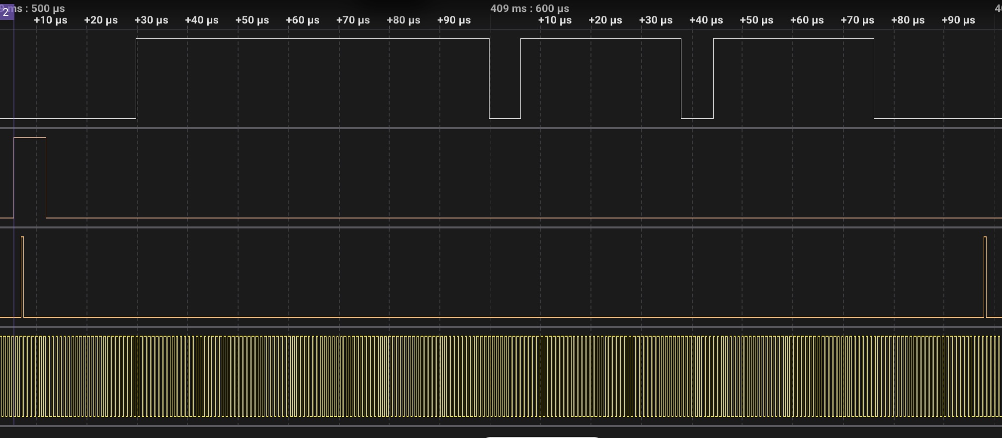
Mapping these 4 signals to the pins above (we skip #3 because it is not used):
The whole image we see on the display must be carried by these 4 signals, which is kind of intimidating. How do we find a picture in these wiggles? Let’s start again with what we know.
The pixels are either black or “white” (amber/blank) so each one probably corresponds to 1 bit in the data coming in. If I use my logic analyzer to count the number of transitions in the likely-clock in between the fast pulses (the third row in the logic analyzer trace) I see there are 240 transitions. Great! That lines up with our 80x3=240 column count guess from earlier. So there is probably 1 row of pixels in-between each of these fast pulses. And that also implies that the fast pulse is probably our LOAD signal, because you would want to LOAD after sending a complete row so it shows up on the screen.
But what about the row driver? It must have something to do with the remaining signal - the second row in the trace. If I count the LOAD pulses that happen between the pulses in the row 2 signal I see that there are 64 of them. Maybe that means there are 64 rows? That matches up with the display aspect ratio perfectly, if we say there are 240 columns. Also computers like the number 64. So row 2 is probably the data line for the row driver. But something is weird. Where is the clock for the row driver? We have used up all of our signals.
To figure this out I went back to the physical circuit board and buzzed out the connections with a multimeter. For each of the 4 signals I put one probe on the connector pin and then dragged the other probe along the pins on the chips until I got a beep indicating a connection. By doing this I confirmed that pin 1 is serial data in (SDI) on the driver chip furthest from the connector. Pin 2 is the data input on the row driver (called DIO1 in the datasheet). Pin 5 is the clock (CP) on all of the 3 column drivers.
Pin 4 had a surprise. It’s connected to LOAD on all of the column drivers like we expected. But it’s also connected to the clock (CP) on the row driver. Now everything makes sense! Here are the steps to update the display:
With our newfound understanding we have some new powers. First, we can take the data about the signals the logic analyzer captured, dump it to a CSV, and then use a Python script to turn it into an image:

Second, we can build our own driver electronics to put an image on the screen:
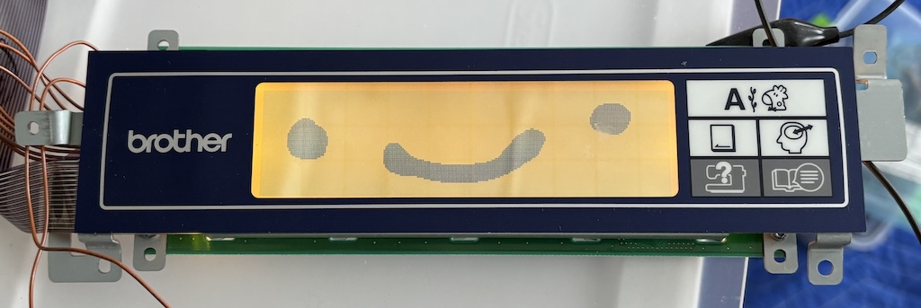
In a future post I’ll get into implementing the driver for my control electronics, but the current status is that I built a PoC using an Arduino Uno to render the smiley doodle above. Then I used my Glasgow Interface Explorer to build a better FPGA version which doesn’t flicker and has a nicer interface for the eventual control MCU to use to display graphics.
Comments
To leave a comment, you need an Are.na account. Comment on this post’s Are.na block and it will appear here.